
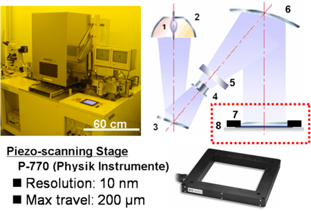
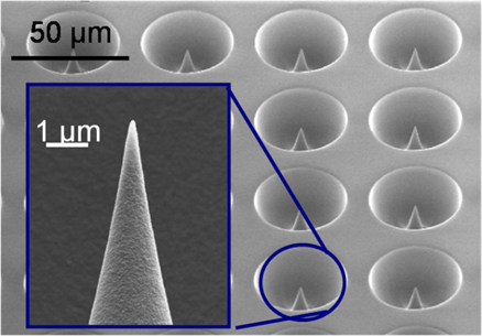
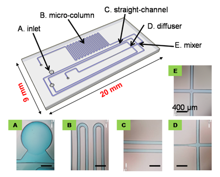
In this study, we proposed a novel 3D (three-dimensional) UV lithography apparatus for thick-film resist and a UV lithography process simulation tool for 3D microstructuring. In order to realize a various 3D microstructures, the developed proximity 3D photolithography apparatus adopts the ‘moving mask lithography’ concept which was originally proposed by Tabata Lab. The moving-mask UV lithography technique is a promising technique for extending the capability of 3D microstructuring since it is possible to realize 3D microstructures with controlled sidewall profile and their wafer-level patterning. Furthermore, we proposed a photolithography simulation tool for thick-photoresist adopting the fast marching method algorithm and developed some devices (e.g., microfluidic devices or packaging technologies) with collaborators which was adopted the moving-mask UV lithography technique.
[Papers]
- Yoshikazu Hirai, Yoshiteru Inamoto, Koji Sugano, Toshiyuki Tsuchiya, Osamu Tabata, “Moving Mask UV Lithography for Three-Dimensional Structuring”, Journal of Micromechanics and Microengineering, Vol.17, No. 2 (2007), pp. 199-206.
- Yoshikazu Hirai, Koji Sugano, Toshiyuki Tsuchiya, and Osamu Tabata, “A Three-Dimensional Microstructuring Technique Exploiting the Positive Photoresist Property”, Journal of Micromechanics and Microengineering, Vol. 20, No. 6 (2010), 065005.
- Yoshikazu Hirai, Koji Sugano, Toshiyuki Tsuchiya, and Osamu Tabata, “Embedded Microstructure Fabrication using Developer-Permeability of Semi-Cross-Linked Negative Resist”, Journal of Microelectromechanical Systems, accepted.
[International Conferences]
- Yoshireru Inamoto, Yoshikazu Hirai, Koji Sugano, Toshiyuki Tsuchiya, Osamu Tabata, “Moving-mask UV lithography and embedded microchannels”, 7th International Workshop on High Aspect Ratio Micro-Structure Technology (HARMST2007), Besan醇Mon, France (June, 2007), pp. 31-32.
- Yoshikazu Hirai, Yoshireru Inamoto, Koji Sugano, Toshiyuki Tsuchiya, Osamu Tabata, “Moving-Mask UV Lithography for 3-Dimensional Positive- and Negative-Tone Thick Photoresist Microstructuring”, The 14th International Conference on Solid-State Sensors Actuators and Microsystems (Transducers’07), Lyon, France (June, 2007), pp. 545-548.
- Yoshikazu Hirai, Yoshiteru Inamoto, Koji Sugano, Toshiyuki Tsuchiya, Osamu Tabata, “Modeling of positive-tone type thick-photoresist dissolution and sequential development profile simulation”, APCOT2008, Tainan, Taiwan, 3E1-3.
- Yoshikazu Hirai, Koji Sugano, Toshiyuki Tsuchiya, Osamu Tabata, “3-dimensional positive thick-resist microstructuring adopting wavelength dependency of photoresist property”, EUROSENSORS XXII, Dresden, Germany, pp. 1559-1602.
- Fred van Keulen, Yoshikazu Hirai, Osamu Tabata, “Objective function and adjoint sensitivities for moving-mask lithography”, The 12th AIAA/ISSMO Multidisciplinary Analysis and Optimization Conference, Victoria, Canada, AIAA-2008-5934.
- Fred van Keulen, Yoshikazu Hirai, Osamu Tabata, “Automated optimization of light dose distribution for moving-mask lithography”, EuroSimE 2009, Delft, The Netherlands.
- Yoshikazu Hirai, Koji Sugano, Toshiyuki Tsuchiya, Osamu Tabata, “3-Dimensional Thick-Resist Microstructuring Adopting Wavelength Dependency of Photoresist Property”, HARMST2009, Saskatoon, Canada, pp. 27-28.
- Yoshikazu Hirai, Hideaki Yoshimune, Kazuya Tsujimoto, Koji Sugano, Toshiyuki Tsuchiya, Osamu Tabata, “Microchannel Embedded in Glass-Frit Layer Bonding for Gas-Filled Sealed Cavity”, HARMST2009, Saskatoon, Canada, pp. 153-154.
- Yoshikazu Hirai, Koji Sugano, Toshiyuki Tsuchiya, Osamu Tabata, “Parameter optimization method for fabricating 3D microstructures embedded in single-layer negative-tone photoresist”, Transducers’09, Denver, CO USA.
- Yoshikazu Hirai, Yusuke Nakai, Koji Sugano, Toshiyuki Tsuchiya, and Osamu Tabata, “Embedded Double-Layered Microchannel Fabrication for Microfluidic Devices using Developer Permeability of Negative Thick-Film Resists”, The 24th International conference EUROSENSORS (EUROSENSORS XXIV), Linz, Austria, accepted.