MEMS Nanogap Device
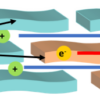
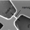
In this research, a single crystal silicon beam was cleaved in a scanning electron microscope(SEM)and current across the cleavagenanogap was measuredto evaluatethe electron transport characteristics. The vacuum nanogaps are expected asahigh-efficiency thermal conversiondevice. However, nanogaps produced by the conventional semiconductor fabrication technologieshave the problemsofsurface roughnessand small opposing area ofand the opposing area ofnm2 order. In order to solve the problem, we have proposed cleavage of single crystal silicon as a method to form nanogaps.We fabricateda nanogap in vacuum and measured the I-V characteristics between pristinefracture surfaces immediately after cleavage and contaminated onesafter air exposure.
[Applications]
- Thermionic conversion device
- Electronic cooling device
【学会発表】
- 文 和彦,霜降 真希,平井 義和,土屋 智由, “単結晶シリコンの真空中へき開によるナノギャップ創成とその清浄破断面間の電界電子放出測定,” 日本機械学会 J22317, 2020.

