
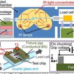
Electrical conduction property measurement of fracture-fabricated silicon nanogap
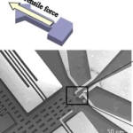
半導体微細加工技術を用いて作製した単結晶シリコンMEMSデバイスの梁構造に(111)面でへき開破壊を用いて数μm角の均一でかつ原子レベルで平滑なナノギャップ構造を作製する技術を確立,電気伝導特性を測定 ...
Tensile testing of silicon covered with DLC film
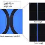
DLC (Diamond Like Carbon) film is one of the promising coating material in MEMS industry deal ...
MEMS Deformable Mirror Actuated By Electrostatic Piston Array
Inspection light of funduscopy is warped by distortion of eyeball. So deformable mirrors (DMs) to co ...
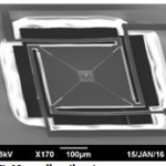
Parallel tensile testing of silicon with integrated strain gauge
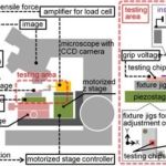
In order to shorten a testing time for evaluation of tensile-mode fatigue properties of single cryst ...
High-temperature mechanical property of single crystal silicon microstructures
Understanding of high-temperature mechanical property is necessary for the reliability of MEMS in ha ...
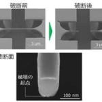
Tensile strength of single crystal silicon microstructures
Silicon is a standard material of MEMS. Since MEMS devices need mechanical deformations for their op ...
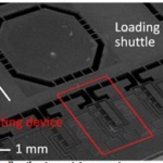
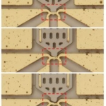
Tensile strength evaluation of free-standing silicon nanowire integrated to MEMS
Silicon nanowire has excellent mechanical and electrical properties and is expected to be app ...
MEMS fabricated conformal electrodes for thermotunneling cooling
A microelectromechanical system (MEMS) is being developed for controlled fracture of a silicon micro ...