Development of Nanopatterning and Reactive Ion Etching of Diamond Film for NEMS Resonator Devices
Nanofabrication technologies have been evolving at an astonishing pace to enable device miniaturization, high integration, high sensitivity, and low power consumption. Nanoelectromechanical Systems (NEMS) integrate nanoscale mechanical components with electronic circuits on a semiconductor substrate. NEMS has various functions such as acceleration sensing, pressure sensing, mass sensing, charge sensing, etc. These technologies are widely applied in fields such as sensing, signal processing, and artificial intelligence. NEMS can play an essential role in our modern lives. Until now, nanofabrication processes have primarily developed around silicon-based semiconductors. However, the growing demand for NEMS devices with superior performance and versatility has driven some research for materials beyond conventional silicon semiconductors.
Diamond, with its unique mechanical, electrical, thermal, and chemical properties, has promised as a superior material for many NEMS applications. Notably, diamond’s biocompatibility and stability in extreme environments open new possibilities for NEMS applications. By developing scalable fabrication processes for diamond NEMS, it may become possible to realize innovative devices for applications in biology, medicine, mining, heavy industry, and planetary exploration. Although some research is conducted for diamond fabrication in microscale, scalable nanofabrication of diamond is not sufficiently studied. In particular, metal nanopatterning on diamond surfaces and etching of diamond for nanostructure formation has not been explored extensively. Achieving scalable diamond NEMS fabrication requires extensive experimental investigations that consider multiple factors impacting these processes.
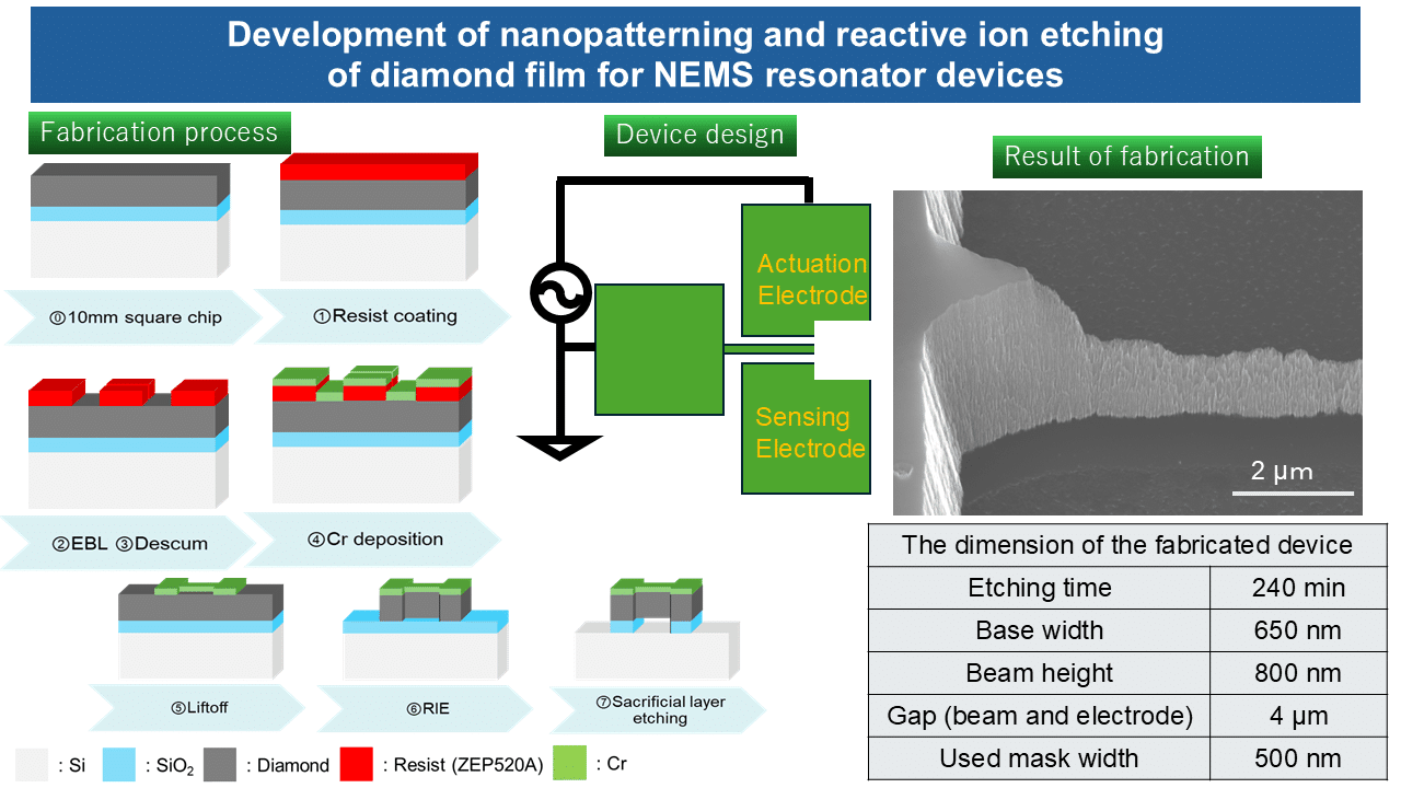
In this study, we develop nanoscale Cr patterning as hard mask by electron beam lithography (EBL) through lift-off process and also reactive ion etching (RIE) of diamond thin film (thickness ~ 2 μm) with O2 plasma to create nanoscale suspended diamond structures for diamond NEMS devices. As a result of this study, we can achieve the nanopatterning of ~ 100nm thickness Cr on diamond film. Additionally, identify the challenges in diamond RIE process for nanofabrication. We report a partial success in creating nanoscale diamond resonators device (beam with a triangular cross-section, a base width of 300–1000 nm and a height of 0.5–1.5 µm, beam length 100–200 µm, gap between beam and electrode is 4 μm) and successfully induce electromechanical oscillation.