MEMSを用いて作製したナノギャップ電極
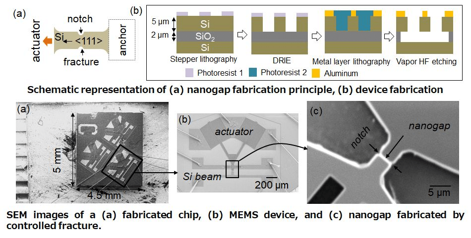
We have developed a microelectromechanical system (MEMS) to fabricate large area nanogap electrodes. A thermal actuator produces a nanogap (~ 100 nm) by controlled fracture of a single-crystalline Si beam (~ 10 x 2 x 5 µm3) (Figures 1a, 2). Flat, parallel, uniform large-area nanogap electrodes have potential applications in:
- Nanoelectronics and molecular electronics,
- Thermotunneling energy harvesting and refrigeration
- Plasmonic and SERS applications
[Fabrication]
The MEMS devices are fabricated from silicon-on-insulator wafer with 5 µm thick, n-type, single-crystalline device layer using stepper assisted photolithography, DRIE, and vapor HF etching of box layer (Figure 1b). Stepper was used to introduce sub-micron size notch on the microbeam to enhance fracture probability.
[Publication]
- A. Banerjee, Y. Hirai, T. Tsuchiya, O. Tabata, Jpn. J. Appl. Phys., 56 06GF06 (2017).
- A. Banerjee, Y. Hirai, T. Tsuchiya, O. Tabata, The 2017 International Meeting for Future of Electron Devices, Kansai (IMFEDK2017), Kyoto, Japan (29-30 June, 2017), pp. 106-107.
- A. Banerjee, Y. Mori, Y. Hirai, T. Tsuchiya, O. Tabata, MRS Fall meeting, Boston, ES09.03.28 (2017).